Following on from my last post, “Designing in the Subthreshold Region with NGSPICE“. In this post I mentioned that unlike designing in the saturation region, device width has little or no effect on device transconductance.
Saturation Region gm
\[ gm= \sqrt{2k’\frac{W}{L}I_{D}} \]
Subthreshold Region gm
\[ gm=\frac{I}{nV_t} \]
Here is a circuit and NGSPICE simulation to demonstrate the point.

Here we have 2 NMOS devices configured as diodes each supplied with 1µA pulsed currents
MN1 has dimensions W=L=2µm so as to be in the saturation region with a 1µA source. MN2 has dimensions W=2µm L= 250nm so as to be in the subthreshold region with a 1µA source
We will now set up an NGSPICE simulation to show the effect of varying device width on both devices.
[box style=”2″ ]
.control
set sourcepath = ( /projects/student/data/netlist/nmos/ )
source nmos_tb.net
save all
save @mn1[vgs] @mn1[vth] @mn1[vds] @mn1[vdsat] @mn1[gm] @mn1[gds]
save @mn2[vgs] @mn2[vth] @mn2[vds] @mn2[vdsat] @mn2[gm] @mn2[gds]
foreach width1 100n, 200n, 400n, 800n, 1.6u
alter @mn1 w = $width1
tran 1n 50n
meas tran D1 find v(drain1) AT=50n
meas tran D2 find v(drain2) AT=50n
let vgst1 = (@mn1[vgs]-@mn1[vth])
let vgst2 = (@mn2[vgs]-@mn2[vth])
plot tran1.@mn1[gm] tran2.@mn1[gm] tran3.@mn1[gm] tran4.@mn1[gm] tran5.@mn1[gm]
plot tran1.vgst1 tran2.vgst1 tran3.vgst1 tran4.vgst1 tran5.vgst1
end
foreach width2 2u, 3u, 5u, 10u, 20u
alter @mn2 w = $width2
tran 1n 50n
meas tran D1 find v(drain1) AT=50n
meas tran D2 find v(drain2) AT=50n
let vgst1 = (@mn1[vgs]-@mn1[vth])
let vgst2 = (@mn2[vgs]-@mn2[vth])
plot tran6.@mn2[gm] tran7.@mn2[gm] tran8.@mn2[gm] tran9.@mn2[gm] tran10.@mn2[gm]
plot tran6.vgst2 tran7.vgst2 tran8.vgst2 tran9.vgst2 tran10.vgst2
end
.endc
[/box]
What’s Going On?
What we are doing here is setting the width of MN1 to 100nm, 200nm, 400nm, 800nm and 1.6µm. Each time we set the width of this device, we run a transient simulation. We then plot the values of gm and Vgst of MN1 for each run.
We then set the width of MN2 to 2µm, 3µm, 5µm, 10µm, 20µm and do as before.
Simulation Results
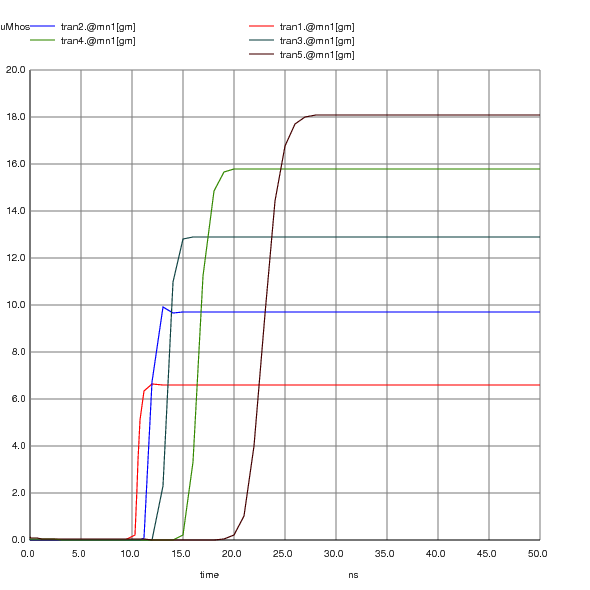
Here are the transconductance and Vgst curves of MN1. Looking first at the Vgst curve, we can see that the looking at the fist run, represented by the red line, through to the last run represented by the brown line, Vgst is above 0V all the time, so we’re in the saturation region.Only just in the case of W=1.6µm.
Looking at the transconductance curves for this device, we see that varying the width of the device changes the transconductance from ~6.5µS to ~18µS. So for a 16X increase in width, we see a 3X change in transconductance

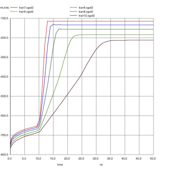
Here are the transconductance and Vgst curves of MN2. Looking first at the Vgst curve, we can see that the looking at the fist run, represented by the red line, through to the last run represented by the brown line, Vgst is below 0V all the time, so we’re in the subthreshold region.
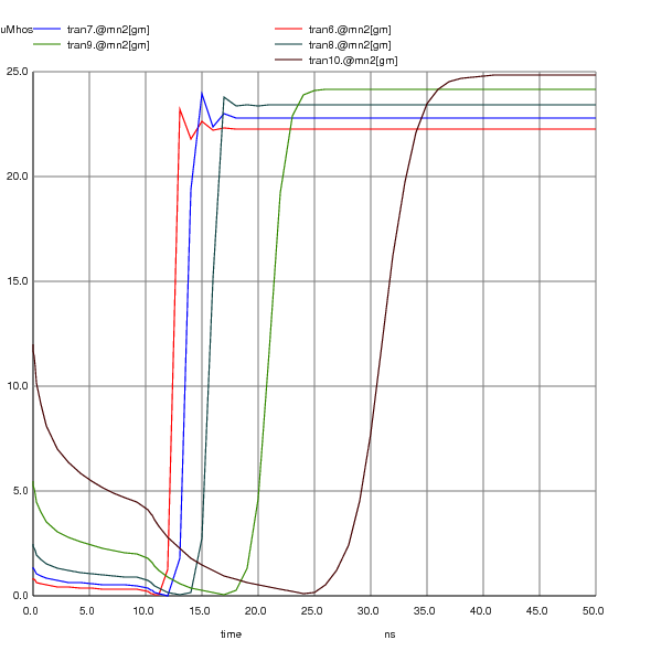
Looking at the transconductance curves for this device, we see that varying the width of the device changes the transconductance from ~22.5µS to ~24.8µS.
In this case the width of the last run is 10X that of the first, yet we see almost no change in transconductance at all.
[profile name=”Justin Fisher” role=”CEO Ingenazure LLC” twitter=”https://twitter.com/ingenazure” facebook=”https://www.facebook.com/ingenazure” linkedin=”https://www.linkedin.com/company/ingenazure” ]Ingenazure LLC[/profile]
