Following on from my last post, “Designing in the Subthreshold Region with NGSPICE“. In this post I mentioned that unlike designing in the saturation region, device width has little or no effect on device transconductance.
Saturation Region gm
\[ gm= \sqrt{2k’\frac{W}{L}I_{D}} \]
Subthreshold Region gm
\[ gm=\frac{I}{nV_t} \]
Here is a circuit and NGSPICE simulation to demonstrate the point.
NMOS Test Bench
Here we have 2 NMOS devices configured as diodes each supplied with 1µA pulsed currents
MN1 has dimensions W=L=2µm so as to be in the saturation region with a 1µA source. MN2 has dimensions W=2µm L= 250nm so as to be in the subthreshold region with a 1µA source
We will now set up an NGSPICE simulation to show the effect of varying device width on both devices.
[box style=”2″ ]
.control
set sourcepath = ( /projects/student/data/netlist/nmos/ )
source nmos_tb.net
save all
save @mn1[vgs] @mn1[vth] @mn1[vds] @mn1[vdsat] @mn1[gm] @mn1[gds]
save @mn2[vgs] @mn2[vth] @mn2[vds] @mn2[vdsat] @mn2[gm] @mn2[gds]
foreach width1 100n, 200n, 400n, 800n, 1.6u
alter @mn1 w = $width1
What we are doing here is setting the width of MN1 to 100nm, 200nm, 400nm, 800nm and 1.6µm. Each time we set the width of this device, we run a transient simulation. We then plot the values of gm and Vgst of MN1 for each run.
We then set the width of MN2 to 2µm, 3µm, 5µm, 10µm, 20µm and do as before.
Simulation Results
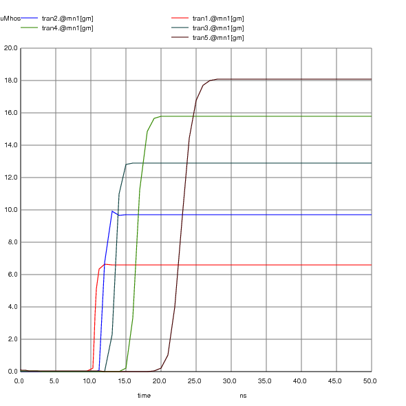
Here are the transconductance and Vgst curves of MN1. Looking first at the Vgst curve, we can see that the looking at the fist run, represented by the red line, through to the last run represented by the brown line, Vgst is above 0V all the time, so we’re in the saturation region.Only just in the case of W=1.6µm.
Looking at the transconductance curves for this device, we see that varying the width of the device changes the transconductance from ~6.5µS to ~18µS. So for a 16X increase in width, we see a 3X change in transconductance
Vgst MN1gm MN1
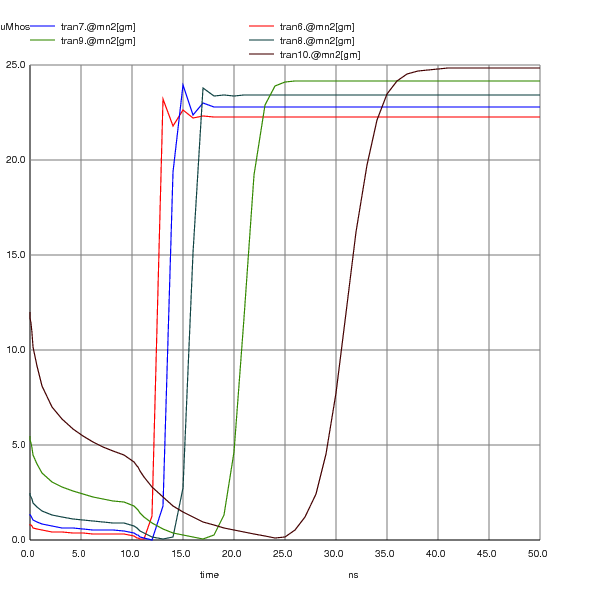
Here are the transconductance and Vgst curves of MN2. Looking first at the Vgst curve, we can see that the looking at the fist run, represented by the red line, through to the last run represented by the brown line, Vgst is below 0V all the time, so we’re in the subthreshold region.
Looking at the transconductance curves for this device, we see that varying the width of the device changes the transconductance from ~22.5µS to ~24.8µS.
In this case the width of the last run is 10X that of the first, yet we see almost no change in transconductance at all.
The subjects of posts here will largely be in response to questions I’m asked by junior engineers. As ever, any material I post will be related to NGSPICE.
With the increased demand for low power, portable applications and the ever shrinking geometry of advanced MOS processes, we see more and more publications regarding sub-threshold design. For engineers, both junior and senior who have never dealt in subthreshold circuit design before, the temptation is to assume that either it’s not so different to normal MOS design in the saturated region or it’s to be avoided at all costs. Neither is correct.
Subthreshold Design Challenges
As for the design challenge aspect of subthreshold versus saturation design, whilst things look the same circuit wise, the way the choices are made regarding device size is completely different.
meaning we can use drain current, gate width and gate length to adjust the voltage gain. This turns out not to be the case in in subthreshold design. In subthreshold MOS devices, gm and rout are given as:
[one_third][math]gm=\frac{Id}{N.Vt}[/math][/one_third] [one_third]where N is a process constant[/one_third] [one_third_last][math]Ro=\frac{1}{\lambda.Id}[/math][/one_third_last]
and Vt is the thermal voltage ~ 26mV at room temperature
meaning the ONLY design variable we have is gate length. Further more gain is inversely proportional to temperature. As an aside, compare the last equation to the gain of a bipolar transistor:
[math]Av = gmRo = \frac {VA}{Vt}[/math]
The MOS device is behaving like a bipolar!
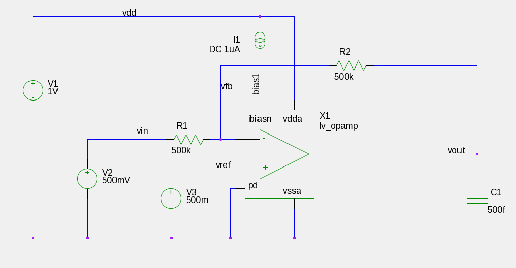
Consider the following opamp circuit:
Low Voltage Opamp
In this case, we will assume that we are working at a company with its own fab. The fab is just bringing up its 90nm process which contains for now only low voltage (core) CMOS devices. The challenge is to design a simple 2 stage miller compensated opamp that is unity gain stable, inverting, with a 500K feedback resistor and driving a 500ff capacitive load.
We are given a bias current of 1µA and a current consumption budget of > 20µA at room temperature.
For the record, I’m not advocating this design as something I’d recommend for a real chip for various reasons, but it is simple, easy to explain and suits the aim of discussing NGSPICE.
The voltage sources are in this schematic in order to measure current. All sources are set to 0V.
First we will use a dc sweep analysis to check our opamp gain.
Low Voltage Opamp DC Sweep Test Bench
Here we sweep the input voltage from 0 to 1V. VDD is also set to 1V.
We are interested in how the small signal parameters of the devices behave as we sweep the input voltage. In oder to do this and referring to the circuit diagram we add the following to our control file.
[box style=”1″]
save all
save @m.x1.mn7[vgs] @m.x1.mn7[vth] @m.x1.mn7[vds] @m.x1.mn7[vdsat] @m.x1.mn7[gm] @m.x1.mn7[gds]
save @m.x1.mn2[vgs] @m.x1.mn2[vth] @m.x1.mn2[vds] @m.x1.mn2[vdsat] @m.x1.mn2[gm] @m.x1.mn2[gds]
save @m.x1.mn5[vgs] @m.x1.mn5[vth] @m.x1.mn5[vds] @m.x1.mn5[vdsat] @m.x1.mn5[gm] @m.x1.mn5[gds]
save @m.x1.mp2[vgs] @m.x1.mp2[vth] @m.x1.mp2[vds] @m.x1.mp2[vdsat] @m.x1.mp2[gm] @m.x1.mp2[gds]
save @m.x1.mp3[vgs] @m.x1.mp3[vth] @m.x1.mp3[vds] @m.x1.mp3[vdsat] @m.x1.mp3[gm] @m.x1.mp3[gds]
save @m.x1.mp7[vgs] @m.x1.mp7[vth] @m.x1.mp7[vds] @m.x1.mp7[vdsat] @m.x1.mp7[gm] @m.x1.mp7[gds]
save @m.x1.mp8[vgs] @m.x1.mp8[vth] @m.x1.mp8[vds] @m.x1.mp8[vdsat] @m.x1.mp8[gm] @m.x1.mp8[gds]
[/box]
What this is doing is saving vgs, vth, vds, vdsat, gm, and gds for the devices we might be interested in looking at.
Save all saves all voltages in the circuits and all currents in voltage sources. It does not however save device small signal parameters. If you need to know the exact syntax of the device small signal parameter you might be interested in you can add the following line to your control deck
display all
Now we have this information we can create some definitions.
[box style=”1″]
let rout1 = 1/(@m.x1.mn5[gds]+@m.x1.mp2[gds])
let rout2 = 1/(@m.x1.mn7[gds]+@m.x1.mp3[gds]+2e-6)
let GM1 = (@m.x1.mn2[gm])
let GM2 = (@m.x1.mp3[gm])
let av1 = 20*log(GM1*rout1)
let av2 = 20*log(GM2*rout2)
let av = av1+av2
let vgst_mn7 = @m.x1.mn7[vgs]-@m.x1.mn7[vth]
let vgst_mp3 = @m.x1.mp3[vgs]-@m.x1.mp3[vth]
let vgst_mn5 = @m.x1.mn5[vgs]-@m.x1.mn5[vth]
let vgst_mp2 = @m.x1.mp2[vgs]-@m.x1.mp2[vth]
let vds_mn7 = v(vout)
let vds_mp3 = v(vdd)-v(vout)
let vdsat_mn7 = @m.x1.mn7[vdsat]
let vdsat_mp3 = @m.x1.mp3[vdsat]
[/box]
What’s this Doing?
rout1 is the output resistance of the first stage.
rout2 is the output resistance of the second stage. the +2e-6 represents the 500K feedback resistor.
GM1 is the transconductance of the first stage.
GM2 is the transconductance of the second stage
From the above four lines we can create equations for the the gain of the two stages and the overall opamp gain.
vgst_mn7, let vgst_mp3, let vgst_mn5 and let vgst_mp2 are the Vgst’s of MN7, MP3, MN5 and MP2 respectively.
vds_mn7 and vds_mn3 define the drain/source voltages of MN7 and MP3
vdsat_mn7 and vdsat_mp3 define the saturation voltages of MN7 and MP3
Running and Plotting
Adding the following line to our control file will run a dc sweep analysis from 0 to 1V in 5mV increments.
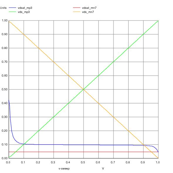
Here we can see he typical operating regions of MP2, MN7 and MN5 are subthreshold, since Vgst’s are below 0V. MP3 is operating in the saturation region.
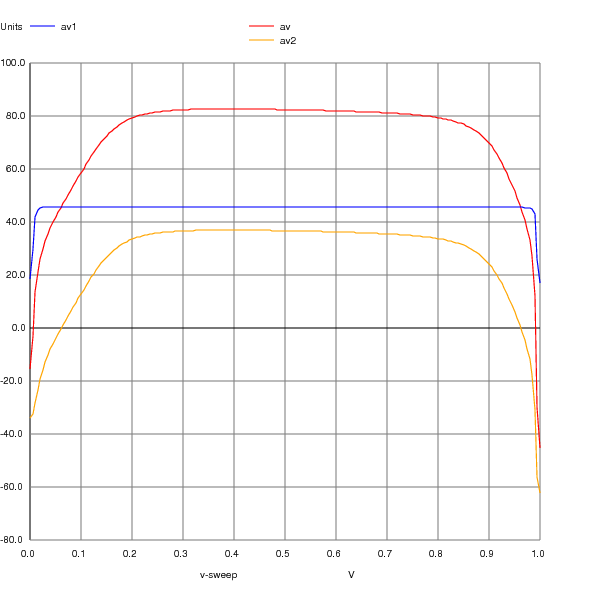
Gain Curves From a dc Sweep
This is interesting. What this is telling us that in the middle of the sweep where perhaps we might be most interested, stage 1 gain is ~45.6dB, stage 2 gain is ~36.7dB giving us an overall gain of 82.4dB.
Another perhaps more interesting aspect is that this graph clearly shows how the dc operating point drastically effects gain. This demonstrates clearly why, when designing an opamp, one should look at stability at multiple operating points.
What’s going on here is that at zero volts input, with vout at its maximum, MN7 is in the triode region. Due to the interaction of the output resistance of MN7 and the feedback network, MN7 is unable to pull vout to VDD. This causes an offset of about 5mV at the input which in turn causes the output of Stage 1 (s1) to pull almost to ground as the loop tries in vain to pull the output up to the rail. As Vin increase, the current at the output required to keep the loop steady reduces. MN7 gradually comes out of the triode region, the offset reduces and the gain of stage 1 rises to its nominal design value.
As the input voltage rises the the positive supply rail, the output voltage tries to fall to zero. In this case, the loop tries to pull the output of the first stage (s1) all the way to the rail in order to cut off MP3. MN7 enters the triode region at Vin ~950mV meaning the output voltage is limited by the source/drain resistance of MN7 and the feedback network.
Once again all this can be visualized in NGSPICE.
[box style=”1]
let vds_mn7 = v(vout)
let vds_mp3 = v(vdd)-v(vout)
let vdsat_mn7 = @m.x1.mn7[vdsat]
let vdsat_mp3 = @m.x1.mp3[vdsat]
plot vdsat_mn7 vdsat_mp3 vds_mn7 vds_mp3
[/box]
VDS VDSAT of MN7 and MP3
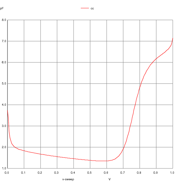
As you recall, this theoretical process contains only low voltage NMOS and PMOS devices. This means we are forced to compensate the amplifier with a MOSCAP. In this case, most, though not all of the MOSCAP value can be seen by looking at CGG in the small signal model
[box style=”1]
let cc = @m.x1.mp7[cgg]
plot cc
[/box]
Compensation Cap Approximation
Which looks really nasty! Another reminder if one were needed that ac or stability analysis should be carried out over a range of operating conditions.
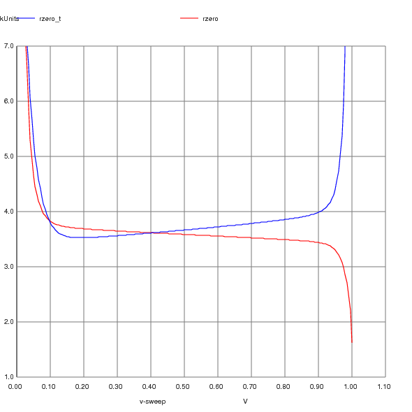
Another thing we can do is visually compare the 1/gm of MP3 to the 1/gds (rds) of the RHPZ compensation device MP8. This allows us to adjust the size of MP8 to get the correct value to cancel out the right half plane zero.
RHPZ GDS and GM_MP3
The Proof of the Pudding!
At this point we’ve carried out a DC sweep analysis on a low voltage opamp using NGSPICE and we have ascertained that the open loop gain should be 82.4dB and the first stage gain 45.6dB for an inverting opamp with Rfb = 500k, VDD=1V and Vin=Vref=0.5V. We can do an AC analysis to see how this correlates.
echo “—-”
echo “—-”
meas ac open_loop_gain find vdb(vout) at=1
meas ac stage_1_gain find vdb(x1.s1) at=1
meas ac dominant_pole when phase=135
meas ac gm_db find mav when vp(vout)=0
meas ac pm_deg find phase when vdb(vout)=0
meas ac pole_2 when phase=45
meas ac gbwp when vdb(vout)=0
Stage 1 gain is indeed shown to be 45.6dB while the open loop gain is shown to be 82.2dB, so we have successfully adjusted the gain a 2 stage opamp using nothing but a DC sweep.
We can now use this analysis technique along with AC and/or STB analysis to optimize the design.